The trend toward increasingly smaller and more complex components in ever-widening variations continues, due to which the greatest amount of test coverage in Electronics production is unavoidable to maintain the highest level of quality. The days when a single test procedure was adequate have long since passed. Zollner Elektronik AG understands the importance of an optimal test strategy.
The constantly growing portion of electronics in and their significance to the functional capability of modern products make an adequate test strategy a prerequisite in the production framework. The main influencing factors here are complexity and in particular the quality and reliability requirements for the respective product.
An optimal test strategy begins in development
If within the scope of development it is it is provided for that a circuit functions within its specified values, a series of test/inspection criteria results, which must be monitored. Among these are specified components, material-dependent characteristic variables as needed, correct installation position and completeness of all connections. In light of the numerous components in a circuit, each with an applicable number of parameters, 100% receiving inspection is neither economically viable nor sensible from a technical effort standpoint. Thus a graduated concept must be applied that combines the various elements in an ideal way. This is ensured especially in the case of electrical testing by DfT analysis (Design for Testability). With this analysis of the circuit diagram, the networks that must be contacted are determined. This is then compared with the physical contact options on the PCB. A test strategy typically encompasses the following steps:
- checking the identity in Receiving and guaranteeing traceability of the entire manufacturing process.
- automated, machine-supported, optical inspection for completeness, correct positioning, the correct quantity and quality of solder joints, short-circuits (soldered jumpers)
- electrical measurement of component element values and circuit parameters (such as the voltage level)
- functional testing of parts or the entire electronics.
Optical inspection systems for early defect recognition
After the identity check in Receiving, typically the first production step is solder paste printing for SMT production. This is decisive for complete soldering of all component connections, therefore the first automated optical inspection is often added at this stage - SPI (Solder Paste Inspection).
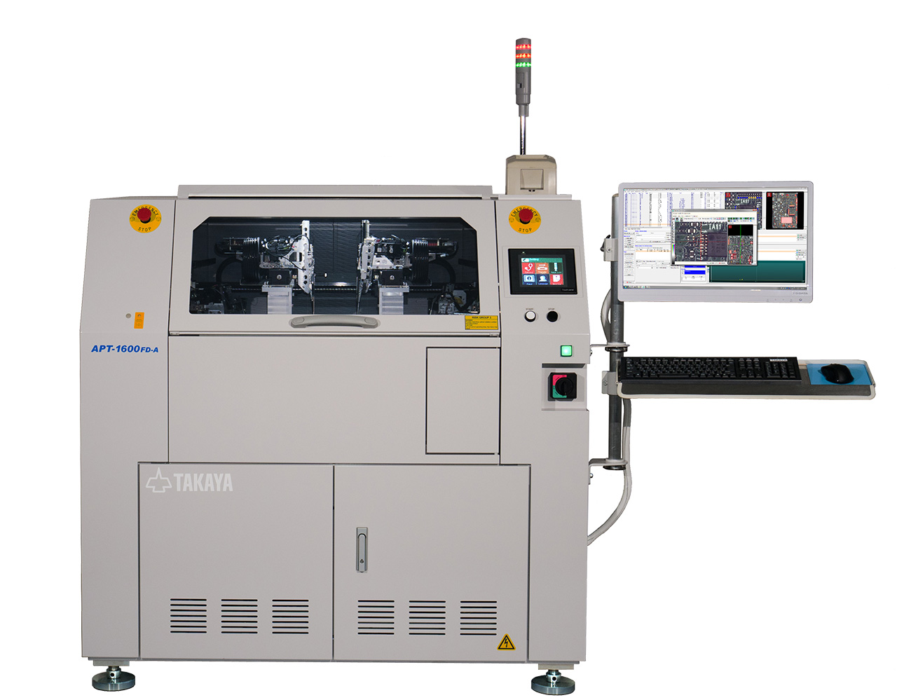
Afterwards follows placement of the components, whereby with active traceability, a modern placement system always <<knows>>, which component from which manufacturer’s lot is to be placed at which installation point. After placement, soldering takes place in a reflow oven - ideally followed by an automated in-line check using AOI/AOXI (Automatic Optical/X-ray Inspection). This checks the completeness of placement, polarity of components - if this can be recognized with marking or shape - as well as completeness and quality of the solder joints (using X-ray, also of BGAs with otherwise invisible solder joints under components.
With complex assemblies of hundreds of components and a number of connections that can quickly climb over the 10,000 mark, automated image data processing is almost mandatory to ensure a short control loop for process malfunctions (and with that prevent scrap). Normally, so-called THT components (Through Hole Technology) follow placement and soldering, but their percentage is constantly being reduced due to advancing miniaturization.
Process optimization based on electrical testing/inspection methods
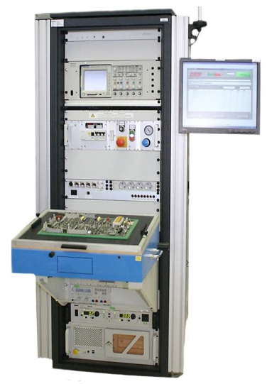
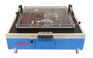
Now electrical testing/inspection is performed on the finished electronics - from FPT (Flying Probe Test), ICT (In-Circuit Test) and Boundary Scan to functional testing. With the Flying Probe Test, program-controlled test pins move over test points or component pads in the circuit and perform individual electrical measurements. The advantage of this procedure is the extreme flexibility and high level of test coverage for simple measurements because the pads can also be reliably contacted. The disadvantage comes from the necessary longer test times due to serial approaches.
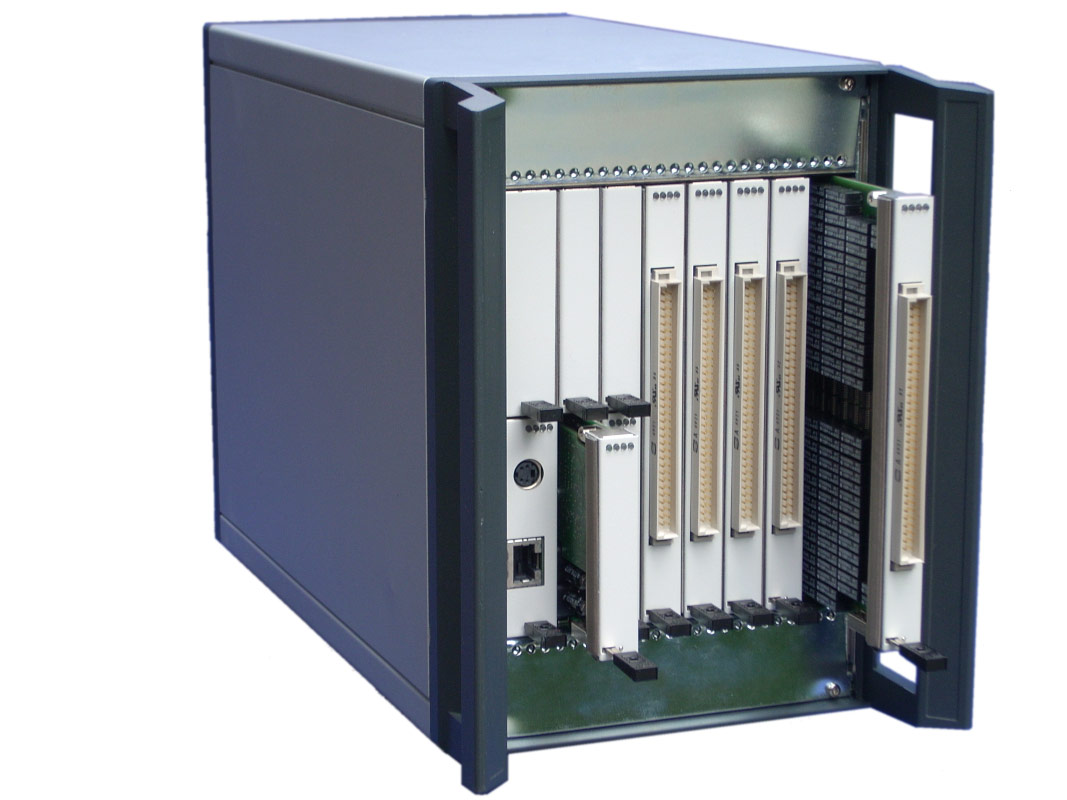
For larger piece quantities - which means less probability of change - ICT (In-Circuit Test) is typically chosen. With ICT, numerous test points are contacted simultaneously, and applicable measurements are also performed, all controlled by a program. Because more test points can be accessed simultaneously with ICT, additional and more complex measurements can be performed than with FPT - all the way to inputting test vectors. ICT advantages over FTP are the higher level of test coverage and the significantly shorter testing time. The disadvantage is higher initial costs in the form of product-specific test fixtures.
Because with modern circuits and constantly increasing packing density, not all circuit points relevant for an electrical test can be contacted, the Boundary Scan Procedure was developed and internationally standardized. This procedure uses integrated cells in special electronic components through which (boundary) signals can be fed into the circuit from the outside. These run through predefined paths within the circuit and are being checked along the way (scanned). With that, the structural integrity of signal paths within a circuit is verified. This can also lead to less contacting effort compared with ICT, but a prerequisite is an applicable test mechanism in the circuit (cells, ports) or components that are capable of Boundary Scan.
Lastly is actual functional testing (FCT) in which the entire functioning of the circuit is checked - for example by feeding in (product-specific) test vectors (digital) or wave forms (analog) and measurement and classification of the resulting measured results. This test is very specifically tailored to the respective product and requires applicable product knowledge. Thus the test environment (test bed) can only be standardized to a limited extent.
Overview of standard testing procedures
The following table - based on the PPVS principle (presence, Polarity, Value, Solder) - provides an overview of the various testing/inspection procedures. PPVS is also used as a simplified principle within the scope of DFT analyses.
Test system | Presence | Polarity | Electrical properties value | Solder Joints |
SPI | x | |||
AOI (SMD) | x | x | x | |
AOI (THT) | x | x | x | |
AXI | x | limited | x | |
FPT | x | limited | x | to some extent |
MDA | x | x | x | to some extent |
ICT | x | x | x | to some extent |
BScan | x | limited | x | to some extent |
FCT | x | limited | limited | to some extent |
Europe's EMS market leader is best prepared
Due to complexity and reliability requirements and the advantages and disadvantages of each procedure, an optimal test strategy is to be derived, which optimizes the sometimes contrary product and customer-specific requirements for test coverage, test depth and costs. Zollner, as an EMS provider supports its customers here in all phases of product development - from DfT analysis (Design for Testability) and guidelines for test points and all the way to implementation.
Corporate-wide, standardized equipment and routine exchange of experiences ensure state-of-the-art, optimal customer support. With more than 100 AOI/AOXI systems, about 20 Flying Probe systems, more than 200 ICT systems (up to 5,000 networks can be contacted) and several hundred Boundary Scan and FCT systems, Zollner is best equipped with machines and expert operators to implement an optimal, tailored test/inspection strategy for the respective product and associated customer requirements.