
A material selection made always requires appropriate analytics with the same dynamics – what we produce, we also need to be able to analyze.

Analysis and materials technology plays a major role at our company throughout the entire product lifecycle. In-depth knowledge of the materials and processes is essential for the success and reliability of a product. This is particularly true when it comes to the selection and qualification of materials in all phases of development, in production, for product modifications, and in the servicing of parts supplied by third parties as well as those made in-house at Zollner. Extensive expertise is needed, including in areas like material characteristics, resistance to reagents and environmental influences, as well as the technical parameters and accompanying thresholds. We offer you an extensive range and as such are able to create a special added value for you. The integration of expertise in materials and analytics in our in-house production processes enables short-term analyses along the entire value chain.


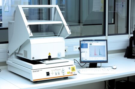
High-resolution detailed examination of samples by means of element analysis for the determination of material compositions (qualitative and quantitative)
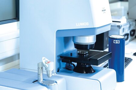
Light microscopy down to the finest detail – metallographic examinations up to 1500-fold or by means of stereomicroscopy up to 115-fold
Material identification of for example, plastics, coatings or residues in minimal quantities – also possible: the analysis of liquids
Measurement of layer thickness/structure and material identification of printed circuit boards and components
Simultaneous multi-element analysis in diverse matrices such as water, wastewater, alloys, etc.

Tracking down particles – evaluation along the process chain, individual parts or functional units and particle traps; evaluations from 25µm with the possibility of material determination of individual particles
Enables components, printed circuit boards, solder joints etc. to be viewed qualitatively and quantitatively from the inside and defects to be illustrated.

Examination of surface resistances to chemicals, re-adjustment of damage cases, general chemical testing
Checking the solderability of components according to standard specifications as a preventive measure and in the event of a fault

Coulometric coating thickness measurement involves measuring the residual thickness of the usable pure tin layer before soldering. This makes it possible to assess the solderability of a tin-coated PCB.

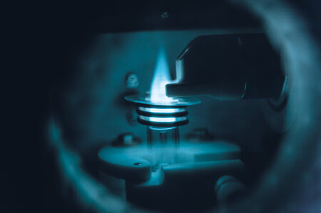
Examination of the thermal behavior in the temperature range from -50°C to 500°C, e.g. to determine melting points, glass transition temperatures
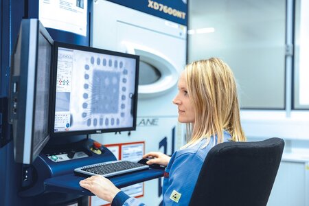
X-ray microscope for non-destructive testing of components, printed circuit boards and assemblies with the possibility of generating 3D models of smaller samples up to a maximum of 5 centimeters in diameter.
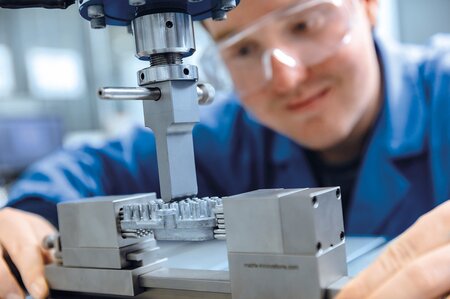
How much can it withstand? – Determination of the strength of materials, joints and components by means of universally applicable and adaptable testing machine

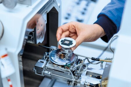
In cases where a direct examination of the chip surface is necessary, for example, to determine the exact version of the chip used or its manufacturer, the chemical opening of electronic components is of vital importance.

Checking the electrical parameters according to the data sheet

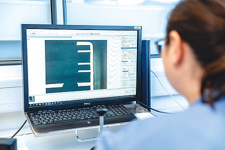
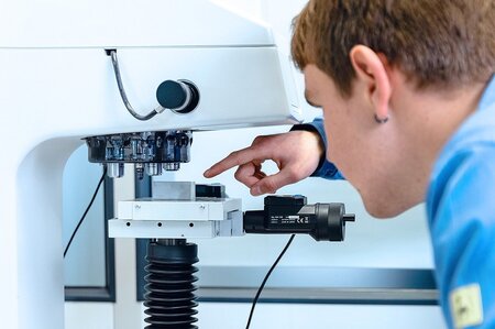
How big is it? – High-precision determination of geometries and dimensions based on 3D models and/or drawings using tactile, optical or non-contact test and measurement.

X-ray analysis, optical microscopic inspection of housings and device markings, electrical testing, acetone abrasion test, and optical microscopic inspection of the inner workings of components with regard to authenticity and proper functioning to rule out counterfeit or damaged components to the greatest possible extent.

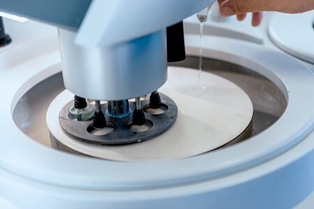
Contact angle measurement using two liquids on surfaces of solids to quantify their wettability – the result makes it possible to make well-founded statements regarding the general wettability of aqueous or organic liquids as well as how their adhesion.
How hard is it? Testing the hardness of metal and plastic samples to check whether they meet the given specifications, for process validation purposes, and for heat treatment purposes in accordance with relevant standards.
